Pci latency timer what value to set. BIOS setup to speed up your computer. BIOS FEATURES SETUP section
- (timeout timer for PCI bus). The value of this option specifies how long (in PCI bus cycles) a PCI card that supports "Busmaster" mode can retain control of the PCI bus if another PCI card is accessing the bus. In fact, this is a timer that limits the time the PCI bus is occupied by the bus master device. After the specified time has elapsed, the bus arbiter forcibly takes the bus from the master, transferring it to another device. The allowable range for changing this parameter is from 16 to 128 in increments of 8. However, in some cases, the "Auto Configured" value (by default) is also added, which greatly alleviates the user's doubts and torments.
The value of the parameter must be changed carefully, as it depends on the specific implementation of the motherboard, and only if the system has at least two PCI cards that support the "Busmaster" mode, for example, a SCSI card and a network card. Graphic cards do not support "Busmaster" mode. The smaller the value, the faster another PCI card that needs access will gain access to the bus. If you need to allocate more time for, for example, a SCSI card, you can increase the value for the PCI slot in which it is located. The value for the network card, for example, should be reduced accordingly or set to 0 altogether, although setting 0 is not recommended in some cases. In general, which value of the parameter is suitable and optimal for a given system depends on the PCI cards used and is checked using test programs. It is also necessary to take into account to what extent "competitor cards" are sensitive to possible delays.
The option may also be called: " PCI Bus Time Out", "PCI Master Latency", "Latency Timer", "PCI Clocks", "PCI Initial Latency Timer". For the last option, the range of possible values was: "Disabled", "16 Clocks", "24 Clocks", "32 Clocks". Another old option, " PCI Bus Release Timer", had the following set of values: "4 CLKs", "8 CLKs", "16 CLKs", "32 CLKs".
And one more very important remark. At one time, this option (and others like it) were introduced taking into account the coexistence of PCI and ISA buses. The ISA bus allowed a single "master" device. This was rarely used before, as it is now. On the other hand, the PCI bus made it possible to simultaneously use several "master" devices. Given the differences in bus speeds, and even more so in their throughput, it was necessary to solve the problem of joint operation of "master" devices on the PCI bus and standard devices on the slower ISA bus. This was especially true of the sound and network cards for ISA-bus, which had a small volume buffer memory, i.e. sensitive to any delays in data transmission. "AMI BIOS" allowed you to select a parameter value in the range from 0 to 255 with a single step. The value "66" was set by default, although a lower PCI device bus ownership was preferred. More recent versions of "AMI BIOS" have become less democratic: 32, 64, 96, 128, 160, 192, 224, 248 and "Disabled". In addition, another option name flashed - " Master Latency Timer (Clks)", and the default value was set to "64".
True, this is not all possible list. Functions " Latency Timer Value" And " Default Latency Timer Value" are applied together. If you set "Yes" in the last option (it is also the default), then the first function will be ignored. A little higher we already talked about the possibility of setting parameters for individual slots. Here's how to implement this feature " Phoenix BIOS":
"PCI Device, Slot #n",
"Default Latency Timer:",
"Latency Timer:",
Naturally, a separate configuration submenu is displayed to work with these parameters. For the nth slot, the user can select the default setting ("Yes"), then the lower field will display the value in hexadecimal form. In this case, the user's access to the "Latency Timer:" field will be blocked. If you set "No" in the "Default Latency Timer:" option, then you will be able to manually set the value from the range: 0000h .... 0280h. The last value corresponds to decimal 640. The default is 0040h (64 clocks).
Another option for the "Latency Timer" option: "20h", "40h", "60h", "80h", "A0h", "C0h", "E0h", "Default" (i.e. "40h") .
Therefore, when solving a specific task (or problem) facing the user, one must first of all proceed from the capabilities of the chipset, BIOS versions and expansion cards used.
End of work -
This topic belongs to:
BIOS Setup Guide
On the website, read: "bios setup guide" ..
If you need additional material on this topic, or you did not find what you were looking for, we recommend using the search in our database of works:
What will we do with the received material:
If this material turned out to be useful for you, you can save it to your page on social networks:
| tweet |
All topics in this section:
CPU Speed 135
4. All about memory 139 Memory monitoring functions 139 Memory shadowing, allocated memory 145 Memory caching 163 Memory regeneration 183
Audio 277
8. Keyboard 280 9. A little about floppy 283 10. Serial and parallel interfaces 285 11. Same
Above 1 MB Memory Test
when the option is set to "Enabled", during the RAM test, a memory area over 1 MB is checked (XMS memory area - Extended Memory Specification). This costs additional
BIOS update
(BIOS update). The P6 family of processors (Pentium Pro, Pentium II, Celeron, Xeon) have a special mechanism called "Firmware" that allows you to fix some of the
Boot Sequence
(system boot sequence). The sequence of polling various drives to boot the operating system is determined. These devices are designated either by letters for physical
Boot Up Floppy Seek
(search for the drive when booting the computer). So you can translate the name of this function. But the meaning of the function is much broader, since the BIOS checks if there is a floppy drive, and whether it is
Boot Up Numlock Status
an option that determines in which mode the additional numeric keypad should work after turning on the computer. Enabling this setting turns on the " Num Lock", and digital key
boot virus detection
(definition of a virus in the boot sector). The meaning of this parameter is different from "Virus Warning" and is as follows. If this parameter is disabled ("Disabled&
CPUID Instruction
not a very clear option. On the one hand, during the POST test, at one of its stages, the CPUID command is executed to obtain the so-called. "CPU Vendor String" and Family/Model/ parameters
Delay IDE Initial
(delay in initialization of the IDE device). This parameter sets the time interval (in seconds) during which the IDE device will not be polled by the BIOS after power on. Nenu
Drive B
using these options, the user sets the specification, format, one might say, the standard of floppy drives used in the system. It doesn't matter if there is a second floppick in
Flash BIOS Protection
- enabling this option prevents viruses and... inexperienced users from accessing the Flash BIOS. However, the contents of the Flash BIOS cannot be updated. To update the function must be disabled. On
Floppy 3 Mode
another, not so rare, option for setting floppy drive parameters. When enabled ("Enabled") allows the system, however trivial, to support 3.5-
Halt On
immediately after turning on the PC, during the POST self-test, if any hardware error is found, the system stops loading and displays the name of the device that caused the failure. Will there be
Keyboard
(keyboard). The value "Installed" does not raise questions. If set to "not installed", this option will tell the BIOS to cancel the keyboard check during the startup test, which will
LAN Remote Boot
- this "Phoenix BIOS" option is noticeably different from the "Boot From LAN First" above. The remote boot feature is particularly useful when neither the floppy drive nor the hard drive
Memory Test Tick Sound
option to accompany the memory test with periodic sound signals. It is recommended to set it to "Enabled" for sounding the download process, an indirect estimate of the volume of the installation
Option ROM Scan
(scanning optional (optional) ROM). An "optional" ROM is a piece of BIOS that can be located on adapter cards and called through the system BIOS to initialize
Processor Number Features
option to set automatic reading and output of information about the built-in serial number processor Pentium III in the BIOS of motherboards that support its installation. To implement such
Quick Power On Self Test
- (a quick test of the computer after turning on the power). Enabling this setting results in some reduction in the initial computer self-test (POST) time, especially with significant
Turbo functions
In ancient times, in Turbo XT and early AT computers, the button< TURBO>on the front of the PC was designed to increase the processor clock speed beyond the nominal for the purpose of
Boot Up System Speed
option to select the processor clock speed at boot. A value of "Low" puts the processor into half-clock mode and does not use the internal cache. Is it true,
Deturbo Mode
- when this parameter is enabled, the FLUSH# signal becomes active, and after that no data is cached into its internal cache by processors of the Pentium Pro architecture (Pentium II, Deschutes, etc.).
CMOS Memory Size Mismatch, Memory Size Changed, memory size has changed since last boot
- volume physical memory on motherboard, determined during the POST test, does not match what is stored in CMOS. Or the message is caused by the memory size changing since last
Missing Operation System
- this message, like some others, is not related to the POST procedure. The output of this message ("Missing operating system") speaks, at best, of the absence or on
Press F1 to disable NMI, F2 to reboot
- problems with non-maskable interrupts. There may be an error in the operation of the interrupt controller, although an error may also occur when checking the memory for parity. This is a non-mask stub handler
NO ROM BASIC - SYSTEM HALTED (AMI)
- indicates a stop in the boot process due to damage or missing boot sector, or master boot record on boot disk. The cause of the error may also be an incorrect setting.
System halted, (Ctrl-Alt-Del) to reboot
- indicates that the download process will stop after a serious error is detected. It is necessary to restart the PC by simultaneously pressing the three indicated keys or by turning the power back on. In
KEYBOARD ERROR OR NO keyboard present
- keyboard error or keyboard missing. All actions are similar. It is also necessary to make sure that no key is pressed when turning on the PC, and also check that the current
Floppy disk(s) fail (40)
- this message at the end of the PC test speaks of possible error in the loop connection. A continuously lit indicator also indicates an incorrect connection. The error may also lie in
Error initializing hard drive controller, HDD Controller Failure, Hard Disk Controller Failure, Fixed Disk Controller Failure, Hard Disk(s) fail (40)
- communication error with the controller hard drives, hard disk controller does not initialize, controller failure. Check the installation of the controller, the connection of the drive, the connection of the
hard disk install failure
- cannot find or initialize the controller or itself HDD. The actions are the same, i.e. check all mechanical settings and connections, as well as correct settings in "BIOS Setup"
Configuration error, x Storage Extensions(s) found, configured are y SE(s)
Device List: k1, k2 ... - mismatch of "Server menu - Storage Extensions" settings found communication devices, where: SEs - storage
chipset
Auto Configuration This mode, when enabled ("Enabled"), allows the system to independently determine the optimal setting of the chipset parameters. Under Optima
Chipset Special Features
- (special features of the chipset). This option enables/disables all new features introduced in Intel 430 kits (HX, VX or TX) compared to FX. If set to "Disabled"
PCI interface and ISA bus
8 Bit I/O Recovery Time (recovery time for 8-bit I/O operations). The parameter is measured in system clocks and determines what delay the system will set.
Optimization of the main and video memory
CPU Burst Write option to enable/disable burst writing to main memory. In normal mode, a separate address is issued for each written word, in block mode, for the entire packet,
Chipset Special Commands
Drive NA before BRDY When "Enabled" is selected, the NA signal (read below) is set one clock before the last BRDY# signal in each read/write cycle, thus calling
CPU Speed
The material in this subsection is built in accordance with standard user actions: setting the system bus clock frequency + setting the multiplier (factor multiplied
Turbo Mode (75 MHz)
- a special option "AMI BIOS", intended for the operation of the Pentium II processor on a 75-MHz system bus. When setting the option to "Disabled", the standard
ECC, Parity
Dynamic memory devices have one serious drawback - the probability of an error in reading information from a cell. Memory errors are detected and corrected using
X ISA LFB Base Address
- this option has no parameters and is for informational purposes only. Shows the main address of the LFB if the size is set in the previous function. ISA Shared Memory Size - (size of ra
X ISA Shared Memory Base Address
- (base address of ISA shared memory). The option is available when the previous function is enabled. This sets the starting address of "ISA Shared Memory". Optionally installed C8000h,
KB to 1MB Cacheability
option via setting to "Enabled" allows you to cache the last 384 KB from the first megabyte of RAM. In the previous chapter and in the options presented below, are quite fully set out in
Ext BIOS EC00-EFFF
Pretty impressive. And here are the values of these options: "PCI Device" - the selected range is given to the needs of the PCI device, "Shadowed" - the selected range &
Cache Extended Memory Area
to use these options offered by the "Phoenix BIOS", caching must first be enabled in the system, for which the integrated option "Cache&q" can be used.
D400-D7FF
D800 - DBFF DC00 - DFFF The values of these options are standard: "Enabled" and "Disabled". Enabling any option causes caches
Cache Timing
- if only one asynchronous cache memory module is installed in the system, then "Fast" must be selected. The "Fastest" value is set if there are two banks in the system
CPU External Cache
- (external processor cache). This option enables/disables the use of the processor's external cache (the second-level cache, or "L2"). Any type of cache should only be disabled
CPU Internal Cache
- (internal processor cache). This option enables/disables the use of the processor's internal cache (the first-level cache, or "L1"). It is worth recalling that the internal cache has become a
Internal Cache WB or WT
- a very old option from "AMI BIOS". Well, its meanings are visible from the name: "WB" (Write Back) and "WT" (Write Through). Sometimes a third value can also be present - &
L2 Cache Cacheable Size
- this option sets the size (amount) of cached memory supported in the system. Values can be: "64 MB", "128 MB", "192 MB", "256 MB"
Shadow Memory Cacheable
- (caching "shadow" memory). An option that allows you to enable the caching mode for those memory areas for which the "shading" mode is already enabled. Option wears an integrated (
System BIOS Cacheable
- (caching of the system BIOS area). Enabling this setting causes a region of memory at system BIOS addresses (F0000H-FFFFFH) to be cached. Enabling the bu option
Tag Options
- the option offers two values for selection. One of them, equal to 8 bits, does not imply the use of the so-called. "dirty" bit. The second allocates 7 bits for the tag itself and one more bit for the pr
Tag Ram Includes Dirty
- the value "Enabled" is not objectionable, because the use of an additional "dirty" bit is intended to improve system performance. Well, what about "Disabled"
Video BIOS Cacheable
- (caching of the video card BIOS area). Enabling this setting causes the memory area at video card BIOS addresses (C0000H-C7FFFH) to be cached in the processor cache. Boo parameter
Video Memory Cache Mode
(caching mode for video memory). The parameter is valid only for Pentium Pro architecture processors (Pentium II, Deshutes, etc.), for which the second-level (L2) cache has become internal. K usually
Refresh
Three different data regeneration methods are possible. Regeneration by one RAS (RAS Only Refresh - ROR). This method was used in the first DRAM chips. Address regenerate
Hidden Refresh
- (hidden regeneration). When set to "Disabled", the memory is refreshed using the IBM AT methodology, using processor cycles for each refresh. When "Hidden Refresh"
DRAM-Config
Auto Configuration option for automatic configuration of main memory access parameters. The option is usually found under "Advanced Chipset Setup" or &qu
Video Config
In modern integrated chipsets, memory is divided by various methods. This can happen due to the software division of the main memory under constant
X RAS to CAS
- "Override" (RAS to CAS delay equals 2 cycles) and "Default" values (delay is determined by the "CAS# Latency" bit (196). The option may be called "RAS-to-CAS
Arbitration, Bus-Master
bus master (bus master, master) - a possible mode of operation of the device on any bus, including PCI. To operate in this mode, the device issues a request to the bus arbiter, reporting
PCI Bus Arbitration
The parameter can take the following values: "Rotating", "Fixed". An option with exactly the same name also met with the parameters: "Favor CPU" and &quo
CPU Priority
after the above, the content of this option may not seem strange anymore. The user must set, in fact, the rank of the CPU in the hierarchy of all possible "master"
Bus Mastering
this option was intended not so long ago to enable or disable the operation of devices in the "Bus-Master" mode on the ISA bus. The parameter can take values: "Enabled"
PCI Bus Parking
- option to enable/disable the "parking" mode of devices on the PCI bus. The "parking" mode is one of the varieties of the "Bus-Master" mode. When this mode is enabled ("E
PCI Mstr Burst Mode
- this option allows you to enable high-speed burst mode for information located in the internal PCI bus write-back buffers, to which the "master" device has access.
State Machines
- the chipset can have four states, more precisely, by controlling the state of its registers, the chipset can have four modes of controlling specific CPU- and/or PCI-operations. Each
All about the PCI bus
PCI (Peripheral Component Interconnect) - 32-bit bus supporting up to ten external devices, provides for data transmission with a clock frequency of 33 MHz and provides ma
PCI 2.1 Support
(support for the PCI bus specification 2.1). When this setting is enabled, PCI bus specification 2.1 features are supported. The 2.1 specification has two main differences from the 2.0 specification: the maximum
PCI Clock Frequency
- option to set the frequency of the PCI bus. In the above form, this option was introduced on the first "Pentium" machines, and then ported to the 486 systems with AMD processors and PCI bus. Cha
PCI Parity Check
some powerful chipsets, primarily server systems, provide the ability (through "Enabled") to control the data flow on the PCI bus by parity. At the same time, they are controlled as an address
PCI Preempt Timer
- (purge timer for PCI bus). At first glance, this function is similar in meaning to the "PCI Latency Timer" function, even some confusion is possible, although in this case something is wrong.
PCI to ISA Write Buffer
- in the "Enabled" state, the system, without interrupting the processor, will temporarily write data to a special buffer for subsequent data transfer to the most suitable mode
Peer Concurrency
- (parallel work or, literally, equal competition). This parameter enables/disables simultaneous operation of several devices on the PCI bus. When this option is enabled, an additional
Init AGP Display First
- when set to "Enabled", the display connected to the AGP-card becomes the primary one in the system. If "Disabled" is selected, then the tone will be set by a PCI card or even ISA.
Multiple Monitor Support
- option to support multiple monitors. There is nothing supernatural in this function. It's even similar to the "Default Primary Video" option, but... This option sets which graphics
Onboard FDC Controller
- an option that determines the use ("Enabled" - by default) or disable the floppy drive controller located on the motherboard, i.e. built-in (onboard). "
Onboard Parallel Port
- this option allows you to disable ("Disabled") the use of the built-in parallel port, automate the process of allocating the required resources ("Auto") or install databases
Onboard PCI IDE Enable
- (enable the integrated IDE controller). This parameter controls the enable/disable operation of each of the two channels of the IDE controller installed on the motherboard. Maybe pr
offboard pci ide card
this "AMI BIOS" option is to enable the IDE interface located on the expansion PCI card. In this case, if an external PCI IDE controller is defined at the initial stage, then the automaton
Secondary Master ARMD Emulated as
Secondary Slave ARMD Emulated as - ARMD (ATAPI Removable Media Disks) are hybrid drives (eg ZIP drives). They are removable, they can be used as floppy
PS/2 Mouse Function Control
- (PS/2 mouse port function control). The permission of this parameter gives IRQ12 only for the PS / 2 mouse port, at the same time it confirms the presence of a mouse with a PS / 2 interface in the system. Otherwise
USB controller
option to enable/disable the USB controller installed on the motherboard. Enabling a USB controller only makes sense if you use the appropriate peripherals. At the same time, the system
USB Keyboard Support
- a similar function, intended in this case to support a USB keyboard. When using such a keyboard, USB controller support must first be activated. If the USB
Resource allocation configuration functions
In 1993, Compaq, Intel, Phoenix, and Microsoft developed the Plug & Play concept to make PCs even smarter.
Configuration Mode
"AMI BIOS" option using "Plug&Play" technology in general configuration of system resources. Can take the following values: "Use BIOS Setup" - the main
Reset Configuration Data
- (reset configuration data). It is recommended to set the option to "Disabled" provided that all connected peripherals and their configuration are constant. When setting "Enabled"
- (how resources are managed). If "Auto" is selected, the BIOS will automatically assign interrupts and DMA channels to all devices connected to the PCI bus, and these options will not appear.
USB IRQ
- (interrupt USB bus). The parameter enables/disables the assignment of an interrupt for the USB bus controller. Since the system may not have enough free interrupt, enable this parameter only
TypeF DMA Buffer Control1(2)
- very interesting "AMI BIOS" option. A normal DMA cycle takes 8 bus cycles, and in this mode- only 3 (which, of course, greatly speeds up access). However, it is necessary
16-bit DMA channel
- select 16-bit DMA channel. Options are: DMA5 (default), DMA6, DMA7. Basic parameters are set. But there are other BIOSes, and hence the different names for similar options:
X Interrupt
- possible values: "IRQ3", "IRQ4", "IRQ5", "IRQ7", "IRQ9", "IRQ10". Audio Output is a very interesting additional o
Keyboard
The keyboards of the first "personal computers" used the 8048 microcontroller. In later models, the 8049 chip with built-in ROM memory or some other
KBC Input Clock
keyboard controller clock frequency control. The parameter sets, in other words, the speed at which the CPU communicates with the keyboard controller. Thus, the parameter
Keyboard Reset Control Typematic Rate Setting X Typematic Rate Delay (msec) Serial, Parallel Port UART2 Mode Select X RxD, TxD Active IR Duplex Mode Parallel Port Mode X ECP DMA Select IDE Prefetch Buffer IDE Secondary Slave UDMA Large Disk Access Mode Video, AGP VLB(VESA) Embedded SCSI BIOS ONB SCSI LVD Term ONB SCSI SE Term SCSI Controller Power Down Functions Hard Disk Timeout standby timeout System shutdown functions System enable functions X KB Power On Hot Key X LAN wake-up mode monitoring temperature monitoring X CPU Critical Temperature MPS 1.4 Support MPS Version Control For OS Spread Spectrum Modulated Server Menu COM Port Address System Event Logging Submenu Mark Existing Events X Pre-Boot Events Password Checking BIOS Reference Data AWARD BIOS The BIOS contains quite a lot of settings, which are not always easy to understand, since help information on some functions is sometimes missing or does not help to clearly understand how they work. Therefore, many users ask a natural question: PCI Latency Timer, what is it? Let's see why this feature is needed and how to set it up correctly. This BIOS setting determines how long a device connected to the PCI bus will hold it for its own use, in order to transfer its data over it. Until this time (number of cycles) has elapsed, all other devices that use the PCI bus will not be able to use it. The default value of this function is 32 or 64 cycles, and in most cases it can be painlessly increased. The minimum value is 32, while the step of the cycle used can be successively increased by 32 cycles (64, 96, and so on), up to 224. Possible Option Values The maximum value of this function can be set to 248. Increasing the PCI Latency Timer value helps to increase the effective bandwidth of the bus of the same name, which in certain cases can lead to incorrect operation of some high-speed devices that transmit and receive large amounts of information. For example, similar problems often occur with RAID controllers. However, it is recommended that you try increasing the value of this setting, especially if your computer has few expansion cards that use the PCI slot. In this case, it is worth gradually (by 32 cycles) increasing the PCI Latency Timer value before the operating system starts loading, and then carefully monitor the performance of the computer and its software. If everything is working properly, then you can consistently increase the PCI Latency Timer value up to about 160 cycles and even higher if there is a serious need for this. On the other hand, if problems occur in the operation of PCI devices, the value of the above parameter should be reduced, down to 64 or even 32 cycles. This need arises when a lot of devices use the PCI bus, some of which need priority access to this bus for error-free operation. Therefore, you should remember that by setting the PCI Latency Timer to 32, you can eliminate such problems. — (timeout timer for the PCI bus). The value of this option specifies how long (in PCI bus cycles) a PCI card that supports the "Busmaster" mode can retain control of the PCI bus if another PCI card is accessing the bus. In fact, this is a timer that limits the time the PCI bus is occupied by the bus master device. After the specified time has elapsed, the bus arbiter forcibly takes the bus from the master, transferring it to another device. The allowable range for changing this parameter is from 16 to 128 in increments of 8. However, in some cases, the “Auto Configured” value (by default) is also added, which greatly alleviates the user’s doubts and torment. The value of the parameter must be changed carefully, since it depends on the specific implementation of the motherboard, and only if the system has at least two PCI cards that support the "Busmaster" mode, for example, SCSI - and a network card. Graphics cards do not support "Busmaster" mode. The smaller the value, the faster another PCI card that needs access will gain access to the bus. If you need to allocate more time for, for example, a SCSI card, you can increase the value for the PCI slot in which it is located. The value for the network card, for example, should be reduced accordingly or set to 0 altogether, although setting 0 is not recommended in some cases. In general, which value of the parameter is suitable and optimal for a given system depends on the PCI cards used and is checked using test programs. It is also necessary to take into account to what extent "competitor cards" are sensitive to possible delays. The option may also be called: "PCI Bus Time Out", PCI Master Latency, Latency Timer, PCI Clocks, PCI Initial Latency Timer. For the last option, a number of possible values looked like: "Disabled", "16 Clocks", "24 Clocks", "32 Clocks". Another old option PCI Bus Release Timer, had the following set of values: "4 CLKs", "8 CLKs", "16 CLKs", "32 CLKs". And one more very important remark. At one time, this option (and others like it) were introduced taking into account the coexistence of PCI and ISA buses. The ISA bus allowed a single "master" device. This was rarely used before, as it is now. But the PCI bus made it possible to simultaneously use several "master" devices. Given the differences in bus speeds, and even more so in their bandwidth, it was necessary to solve the problem of cooperative operation of "master" devices on the PCI bus and standard devices on the slower ISA bus. This was especially true for sound and network cards for the ISA bus, which were common at that time, and had a small amount of buffer memory; sensitive to any delays in data transmission. "AMI BIOS" allowed you to select a parameter value in the range from 0 to 255 with a single step. The value "66" was set by default, although a smaller value of PCI device bus ownership turned out to be more preferable. More recent versions of the "AMI BIOS" have become less democratic: 32, 64, 96, 128, 160, 192, 224, 248 and "Disabled". In addition, another option name flashed - "Master Latency Timer (Clks)", and the default value was set to "64". True, this is not the whole list. Functions Latency Timer Value And "Default Latency Timer Value" are applied together. If the last option is set to "Yes" (it is also the default), then the first function will be ignored. A little higher, we already talked about the possibility of setting parameters for individual slots. Here is how Phoenix BIOS implements this feature: PCI Device, Slot #n", "Default Latency Timer: ", "Latency Timer: ", Naturally, a separate configuration submenu is displayed to work with these parameters. For the nth slot, the user can select the default setting ("Yes"), then the value in hexadecimal form will be displayed in the lower field. In this case, the user's access to the "Latency Timer:" field will be blocked. If you set “No” in the “Default Latency Timer:” option, then you will be able to manually set a value from the range: 0000h ... 0280h. The last value corresponds to decimal 640. The default is 0040h (64 clocks). Another option for the values of the "Latency Timer" option: "20h", "40h", "60h", "80h", "A0h", "C0h", "E0h", "Default" (i.e. "40h") . Therefore, when solving a specific task (or problem) facing the user, one must first of all proceed from the capabilities of the chipset, the BIOS version, and the expansion cards used. - (support for PCI 2.1 bus specification). When this setting is enabled, PCI bus specification 2.1 features are supported. Specification 2.1 has two main differences from specification 2.0: the maximum bus clock frequency is increased to 66 MHz and the PCI-PCI bridge mechanism is introduced, which allows removing the limitation of specification 2.0, according to which no more than 4 devices can be installed on the bus. In addition, the introduction of the 2.1 specification made it possible to optimize the coexistence of PCI and ISA buses (for more details, see the "Delayed Transaction" option). Disabling this setting makes sense only if problems arise after installing an additional PCI card (as a rule, problems can arise only with fairly old PCI devices), as well as with ISA devices that do not want to buffer their information in any way, and therefore also do not support this specification. The parameter can take values: Option to set the frequency of the PCI bus. In the above form, this option was introduced on the first "Pentium" machines, and then transferred to 486 systems with AMD processors and a PCI bus. The bus frequency was "tied" to the CPU frequency through a multiplier and had the following range of values: "CPUCLK/1.5" (by default), "CPUCLK/2", "CPUCLK/3" and fixed "14 Mhz" (it was so!) . Setting to "Enabled" allows the system to remember the PCI command that was just requested. If subsequent commands match some address area, write cycles will be automatically interpreted as PCI commands. - (timeout timer for PCI bus). The value of this option specifies how long (in PCI bus cycles) a PCI card that supports "Busmaster" mode can retain control of the PCI bus if another PCI card is accessing the bus. In fact, this is a timer that limits the time the PCI bus is occupied by the bus master device. After the specified time has elapsed, the bus arbiter forcibly takes the bus from the master, transferring it to another device. The allowable range for changing this parameter is from 16 to 128 in increments of 8. However, in some cases, the "Auto Configured" value (by default) is also added, which greatly alleviates the user's doubts and torments. The option can also be named: "PCI Bus Time-out", "PCI Master Latency", "Latency Timer", "PCI Clocks", "PCI Initial Latency Timer". For the last option, the range of possible values was: "Disabled", "16 Clocks", "24 Clocks", "32 Clocks". Another old option, "PCI Bus Release Timer", had the following set of values: "4 CLKs", "8 CLKs", "16 CLKs", "32 CLKs". Some powerful chipsets, primarily server systems, provide the ability (through "Enabled") to control the data flow on the PCI bus by parity. In this case, both the address data and the actual data are monitored. Errors are not corrected, but the user is informed about them. What is also important is that the PCI expansion card itself must support this method of control. - (purge timer for PCI bus). At first glance, this function is similar in meaning to the "PCI Latency Timer" function, even some confusion is possible, although in this case something is the opposite. The value of this option specifies how long (in PCI bus clocks, or local clocks - LCLKs) a PCI card that supports the "Busmaster" mode can not control the bus, but wait while another card owns this bus. The bus arbiter keeps track of the specified time interval since the request is made, after which the waiting "master" device preempts its "mate". - (parallel work or, literally, equal competition). This parameter enables/disables simultaneous operation of several devices on the PCI bus. When this option is enabled, additional buffering of read/write cycles in the chipset is enabled. But problems can arise if not all PCI cards are ready to support this mode of operation. In this case, the performance of the system is tested empirically. - (timeout timer for PCI bus). The value of this option specifies how long (in PCI bus cycles) a PCI card that supports the "Busmaster" mode can retain control of the PCI bus if another PCI card is accessing the bus. In fact, this is a timer that limits the time the PCI bus is occupied by the bus master device. After the specified time has elapsed, the bus arbiter forcibly takes the bus from the master, transferring it to another device. The allowable range for changing this parameter is from 16 to 128 in increments of 8. However, in some cases, the “Auto Configured” value (by default) is also added, which greatly alleviates the user’s doubts and torment. The value of the parameter must be changed carefully, as it depends on the specific implementation of the motherboard, and only if the system has at least two PCI cards that support the "Busmaster" mode, for example, a SCSI card and a network card. Graphics cards do not support "Busmaster" mode. The smaller the value, the faster another PCI card that needs access will gain access to the bus. If you need to allocate more time for, for example, a SCSI card, you can increase the value for the PCI slot in which it is located. The value for the network card, for example, should be reduced accordingly or set to 0 altogether, although setting 0 is not recommended in some cases. In general, which value of the parameter is suitable and optimal for a given system depends on the PCI cards used and is checked using test programs. It is also necessary to take into account to what extent "competitor cards" are sensitive to possible delays. The option may also be called: " PCI Bus Time Out", "PCI Master Latency", "Latency Timer", "PCI Clocks", "PCI Initial Latency Timer". For the last option, a number of possible values looked like: "Disabled", "16 Clocks", "24 Clocks", "32 Clocks". Another old option, " PCI Bus Release Timer", had the following set of values: "4 CLKs", "8 CLKs", "16 CLKs", "32 CLKs". And one more very important remark. At one time, this option (and others like it) were introduced taking into account the coexistence of PCI and ISA buses. The ISA bus allowed a single "master" device. This was rarely used before, as it is now. But the PCI bus made it possible to simultaneously use several "master" devices. Given the differences in bus speeds, and even more so in their bandwidth, it was necessary to solve the problem of cooperative operation of "master" devices on the PCI bus and standard devices on the slower ISA bus. This was especially true for sound and network cards for the ISA bus, which were common at that time, and had a small amount of buffer memory; sensitive to any delays in data transmission. "AMI BIOS" allowed you to select a parameter value in the range from 0 to 255 with a single step. The value "66" was set by default, although a smaller value of PCI device bus ownership turned out to be more preferable. More recent versions of the "AMI BIOS" have become less democratic: 32, 64, 96, 128, 160, 192, 224, 248 and "Disabled". In addition, another option name flashed - " Master Latency Timer (Clks)", and the default value was set to "64". True, this is not the whole list. Functions " Latency Timer Value" And " Default Latency Timer Value" are used together. If you set the last option to "Yes" (it is also the default), then the first function will be ignored. A little higher, we already talked about the possibility of setting parameters for individual slots. Here's how Phoenix BIOS implements this feature: "PCI Device, Slot #n", "Default Latency Timer:", "Latency Timer:", Naturally, a separate configuration submenu is displayed to work with these parameters. For the nth slot, the user can select the default setting ("Yes"), then the value in hexadecimal form will be displayed in the lower field. In this case, the user's access to the "Latency Timer:" field will be blocked. If you set “No” in the “Default Latency Timer:” option, then it will be possible to manually set a value from the range: 0000h ... 0280h. The last value corresponds to decimal 640. The default is 0040h (64 clocks). Another option for the values of the "Latency Timer" option: "20h", "40h", "60h", "80h", "A0h", "C0h", "E0h", "Default" (i.e. "40h") . Therefore, when solving a specific task (or problem) facing the user, one must first of all proceed from the capabilities of the chipset, the BIOS version, and the expansion cards used.
- option to control the restart from the keyboard. When the option is set to "Enabled" there is standard feature restarting the computer when using a set of keys
- (set character input speed). This option may allow you to eliminate not entirely correct keyboard modes. First of all, you need to set the value of the option to "Enabled" (
- (repeat delay in ms). This option adjusts the second time characteristic - the delay before the auto-repeat of the pressed key, which can vary from 0.25 to 1 second, i.e. delay value
Serial interface Attention!!! With not quite correct behavior of the "mouse" (unstable work, jumps, uneven movement) over
the presence of such an option in "BIOS Setup" means that the motherboard supports the IrDA function. The option itself is "subordinate", since its activation is directly related to the
- option to set the polarity of signals for receiving/transmitting the infrared interface. It is worth mentioning that "RxD" means receiver (receiver), and "TxD" means transmitter (transmitter). For
- option to select full duplex or half duplex mode of the infrared port. The default is "Half". Another meaning is naturally "Full" (duplex)
(parallel port operation mode). Naturally, this option cannot be active if the use of the parallel port is disabled. This parameter allows you to set the operating modes of the parallel port in
- (DMA channel selection for ECP mode). The parameter is activated only when the "ECP" or "ECP+EPP" mode is enabled. Can take the following values: "1" (or, for example, "DMA
(IDE prefetch buffer). The built-in IDE interface supports a prefetch mode, which speeds up reading from the disk buffer, reducing the computer's bus time. On the SiS496 controller
these options allow you to set the mode of operation of each of the four hard drives in the system that support the Ultra ATA (Ultra DMA) specifications. If an EIDE disk is installed in the system (especially an IDE disk),
"Phoenix BIOS" option to control access mode to large capacity disks (more than 1024 cylinders and 16 heads). The option associates disk access with how the operating system
AGP -2x Mode defaults to "Disabled". "Enabled" is selected only if the graphics card supports AGP 2x mode. AGP
The VL-BUS bus, proposed by the Video Electronics Standard Association (VESA), was originally intended to increase the speed of video adapters. The first tire standard would
- this option allows (via "Enabled") to copy the SCSI BIOS of the controller to the system BIOS. The advantages of such a solution are obvious. Otherwise, the BIOS of the SCSI controller will be the system
- (terminators of the built-in SCSI LVD controller). This parameter enables/disables connection of termination resistors (terminators) on the built-in SCSI controller with LVD signaling. "Phoen
- (onboard SCSI SE controller terminators). This parameter enables/disables connection of termination resistors (terminators) on the built-in SCSI controller with SE data transfer. Can accept
- SCSI controller support option. There is nothing unusual about this option, unless you point out that it was intended for ISA boards as well. First of all, the SCSI controller occupies one ISA server.
Hard Disk Power Down Mode - this option sets the conservation (power consumption) mode, which will enter the hard disk after the end of the set period of inactivity
- To use this option, the "Power Management Mode"(336) option must first be set to "Customize" (or "Power Savings" to "Enabled"). Dan
- to use this option, the "Power Management Mode"(338) option must first be set to "Customize" (or "Power Savings" to "Enabled"). Dan
After G3 Enable - this option allows (if set to "Enabled") as a result of switching power saving modes to enter the G3 state, which, according to the method,
AC PWR Loss Restart - (restart after power failure). Enabling this setting allows the system to turn on automatically after a power failure. Otherwise
- when "Hot Key" is selected, the "KB Power On Hot Key" field is activated. The user is offered a choice of one of the options for starting the system using "hot keys &
- the option is available when the previous option is enabled. Through this option, "Phoenix BIOS" allows you to turn on the monitor ("On") when you turn it on remotely. Otherwise - "Off"
The first company that began to use built-in controls in mass models of motherboards was the company "ASUSTeK". One of the leaders in the production of maternal products
- option to enable ("Enabled") the function of temperature monitoring of the system. Fan Monitor Section Chassis Fan Speed CPU Fan Speed
- possible options: "Disabled", "45C", "50C", "55C", "60C", "65C", "70C", "75C". Thermal Sensor State
- support for MPS 1.4 mode (Intel Multiprocessor Specification). This option only appears in the BIOS of motherboards that allow multiple processors. The parameter specifies the operating
- similar option with the following values: "1.4" (default), "1.1". With the same parameters in the "AMI BIOS" options "M
- (distribution of the modulated spectrum). During the operation of the clock generator, a phenomenon such as electromagnetic interference (ElectroMagnetic Interference - EMI) may occur. Physical interface
EMP Password - a server board (for example, C440GX) must have a port called EMP (Emergency Management Port - emergency management port), which is a
- possible options: "Disabled", "3F8" - usually the address of COM1, "2F8" - usually the address of COM2, "3E8". After specifying the address
Along with the configuration submenu of the console, the BIOS of the server motherboard may contain a submenu with the characteristics of various system events. User (administrator) set row
- the purpose of this option is quite simple, but the applicability? The user is prompted to set attributes for all entries in the log; whether they are intended to be read or not. by default
- Fixed errors during POST testing. To work effectively with these menus, it is necessary to rationally use the "On Next Boot" option to clear the log. Choosing l
- "AMI BIOS" option, similar to "Security Option" for "Award BIOS", with the only difference that the "System" value corresponds to the "Always" value, but
Currently, most of the motherboards are equipped with BIOS manufactured by the following companies: - AWARD Software International Inc. (part of Phoenix since 1999)
Version 2.50: AWARD_SW j262 TTPTHA 01322222 KDD ZBAAACA aPAf lkwpeter t0ch88 t0ch20x h6BB j09F Version 2How to set this setting correctly
"Enabled" - allowed,
"Disabled" - prohibited.
The option may be called "PCI 2.1 Compliance". PCI Clock Frequency
The "PCI Clock Speed" option offered the following values: "Same as CPU", "2/3 CPU", "CPU/2", "1/8 CPU". The "HCLK PCICLK" option was a divisor between the system clock and the local bus clock: "1-1", "1-1.5", "AUTO". The "PCI Bus Frequency" option offered the values "CPUExt/3", "CPUExt/2.5", "CPUExt/2" and they linked the PCI bus frequency to the system bus. The "CPU Host/PCI Clock" option allowed the PCI bus to get the standard 33 MHz only through the "Default" value.
The preliminary picture would be incomplete without two joint options. The "PCI Clock Speed Override" option, through the "Enabled" value, generally gave permission to "redefine" the PCI bus frequency, but the "PCI CLK" option could surprise even an experienced user. The "Asynchronous" value made it possible to select an arbitrary frequency for the PCI bus. But the "Synchronise" value "rigidly" linked the clock frequency of the system bus and the frequency of the PCI bus. Only beforehand, with the help of jumpers on the motherboard, it was necessary to set the system frequency and multiplier for the processor and, as a result, get, for example, for Pentium 120 frequencies: 120, 60 and 30 MHz (PCI bus).
A much more modern option is the "PCI/AGP Clock" option. This means that this option sets the frequencies for two buses, although not so long ago various BIOS versions did not provide such opportunities. This version of the option is intended to a greater extent for "overclocking" devices on the PCI bus (very dangerous) and for AGP. Option values, i.e. bus frequencies are directly related to the system bus frequency settings in the "CPU Host Clock" option. If the latter is greater than or equal to 100 MHz, then PCI and AGP are set to "CPU Host Clock"/3 and /1.5, respectively. For a lower processor bus frequency, the division is made by 2 and 1. Therefore, if the system frequency is 66 MHz, then for PCI and AGP we get the standard ratio of 33/66 MHz. The same, i.e. standard, the variant takes place at a frequency of 100 MHz. All other values of the system bus frequency lead to "overclocking" of both interfaces.
Modern systems with options like "System/PCI Frequency (MHz)" provide the widest possibilities for "overclocking", namely not a set of several values, but a solid menu with a number of parameters, starting from the value "100/33" (divider 3: 1) and ending with "178/44.51" (4:1 divider) and in 1 MHz system bus steps. All this would be great if there were no element of risk. Almost all mainboard manufacturers "successfully" began to solve the problem of "overclocking" PCI- and AGP-interfaces, relegating to the last plan the possibility of accelerating the system bus and the processor without "drawing" other system components into this "overclocking". The first "swallow" in this "overclocked" world was the motherboard from "Gigabyte" - GA8IRXP, which offered additional separate dividers for each of the buses and thus made it possible to essentially set the optimal frequencies for the PCI and AGP interfaces, regardless of the "overclocked" system one. PCI Dynamic Decoding
PCI Latency Timer (PCI Clocks)
The value of the parameter must be changed carefully, as it depends on the specific implementation of the motherboard, and only if the system has at least two PCI cards that support the "Busmaster" mode, for example, a SCSI card and a network card. PCI graphics cards do not support the "Busmaster" mode, rather, they did not. The smaller the value, the faster another PCI card that needs access will gain access to the bus. If you need to allocate more time for, for example, a SCSI card, you can increase the value for the PCI slot in which it is located. The value for the network card, for example, should be reduced accordingly or set to 0 altogether, although setting 0 is not recommended in some cases. In the general case, what value of the parameter is suitable and optimal for a given system depends on the PCI cards used and is checked using test programs and trial operation. It is also necessary to take into account to what extent "competitor cards" are sensitive to possible delays. Given the above, let's recall the existence of another "master" device, namely, the central processor. So too low a timeout value can affect the efficiency of local bus processor control.
And one more very important remark. At one time, this option (and others like it) were introduced taking into account the coexistence of PCI and ISA buses. The ISA bus allowed a single "master" device. This was rarely used, both before and in the last years of the existence of the ISA bus. On the other hand, the PCI bus made it possible to simultaneously use several "master" devices. Given the differences in bus speeds, and even more so in their throughput, it was necessary to solve the problem of joint operation of "master" devices on the PCI bus and standard devices on the slower ISA bus. This was especially true for sound and network cards for the ISA bus, which were common at that time, and had a small amount of buffer memory; sensitive to any delays in data transmission.
"AMI BIOS" allowed to select the parameter value in the range from 0 to 255 cycles with a single step. The value "66" was set by default, although a lower PCI device bus ownership was preferred. More recent versions of "AMI BIOS" have become less democratic: 32, 64, 96, 128, 160, 192, 224, 248 and "Disabled". In addition, another name of the option "flickered" - "Master Latency Timer (Clks)", and the default value was set to "64".
True, this is not the whole list. The "Latency Timer Value" and "Default Latency Timer Value" functions are used together. If the last option is set to "Yes" (which is also the default), then the first function will be ignored. A little higher, we already talked about the possibility of setting parameters for individual slots. Here is how "Phoenix BIOS" implements this feature:
"PCI Device, Slot #n",
"Default Latency Timer: ",
"Latency Timer: ",
Naturally, a separate configuration submenu is displayed to work with these parameters. For the nth slot, the user can select the default setting ("Yes"), then the lower field will display the value in hexadecimal form. In this case, the user's access to the "Latency Timer:" field will be blocked. If you set "No" in the "Default Latency Timer:" option, then you will be able to manually set the value from the range: 0000h .... 0280h. The last value corresponds to decimal 640. The default is 0040h (64 clocks).
Another option for the "Latency Timer" option: "20h", "40h", "60h", "80h", "A0h", "C0h", "E0h", "Default" (i.e. "40h") .
Therefore, when solving a specific task (or problem) facing the user, one must first of all proceed from the capabilities of the chipset, the BIOS version, and the expansion cards used.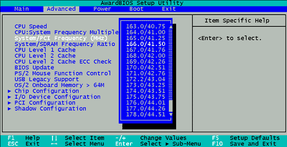
PCI Parity Check
The option may also be called "PCI Parity Checking" or "PCI Bus Parity Checking". PCI Preempt Timer
Values from the range: 5, 12, 20, 36, 68, 132, 260, in digital form or with the display of the unit of measure - "5 LCLKs", etc. are offered for selection. The "No Preemption" (or "Disabled") parameter is required. And the latter, as a rule, is installed by default. This option is no longer used in this form, so encountering it on older machines can cause some difficulties. In any case, if there are at least two "master" devices on the PCI bus, the "Disabled" value (or similar) should be replaced with a more optimal one.
The option may also be called "PCI Preemption Timer". Peer Concurrency
This option also affects the joint operation of PCI and ISA buses. For example, PCI bus cycles can be reallocated and buffered during ISA operations such as DMA bus-master transfers. The parameter can take values:
"Enabled" (default) - enabled,
"Disabled" - prohibited.
The option may also be called "PCI Concurrency" or "Bus Concurrency". Additional "hungry for competition" devices appear in the "PCI/IDE Concurrency" or "PCI-to-IDE Concurrency" options.
PERR#
SERR#
- "AMI BIOS" through the usual "Enabled" (enabled, enabled) and "Disabled" (prohibited, disabled) prompts the user to "work" with the interface signals of the PCI bus: PERR# and SERR#. These signals, for reference, correspond to the bus contacts - B40 and B42, respectively. A few words about the signals themselves.
"PERR#" - I/O PCI Parity Error. The signal is set by the data receiver on the bus one bus cycle after the PAR signal is issued (Parity Error - pin A43). The PERR# signal becomes active if a parity error is detected on the PCI bus. In this case, the "Enable" bit is set in the PCICMD register by the PERR# signal. With this option, you can just disable the installation of an error signal ("Disabled" is set by default).
"SERR#" - I/O PCI System Error. As a result, the "SERRE" (SERR# Enable) bit is also set in the PCICMD register. This is an integrated signal that requires one of the following conditions to be set:
1. The PERR# signal is set on the PCI bus, which is controlled by bit 3 of the ERRCMD register,
2. The SERR# signal will be asserted one bus cycle after a data transfer violation is detected during initiated PCI cycles,
3. The SERR# signal will be set during ECC operations. An ECC error is signaled via the ERRCMD control register for a correctable single-bit error or multiple non-correctable,
4. The SERR# signal will be asserted when a parity error on the PCI bus is detected during the transfer of address data while setting some error signals in other registers,
5. There may be additional situations, such as setting the G-SERR# error input in bit 5 of the ERRCMD register.
 How to Connect Android Devices to TV Connecting via HDMI
 How to install TWRP Recovery on Android - step by step instructions Installing recovery on a tablet
 How to disable Samsung Pay from the screen: bottom and main parts Delete cache and cookies
 Modern types of memory DDR, DDR2, DDR3 for desktop computers
 Smartphones, phones, tablets, laptops, registrars and other mobile electronic devices in assortment at affordable prices with delivery throughout Russia and the CIS
 Driver diagnostics
 RAW processing: how to get the most out of your photos